


How to run thermal and stress simulation on a PCB enclosure in the browser

Flux runs thermal and stress simulation from a text prompt in your hardware project. This walkthrough connects a 50 × 30 mm PCB, its 2 W regulator, and the enclosure that holds it. One thermal-pad change reduced the calculated regulator maximum from 172.94 °C to 57.46 °C in a conduction-only aluminum model.
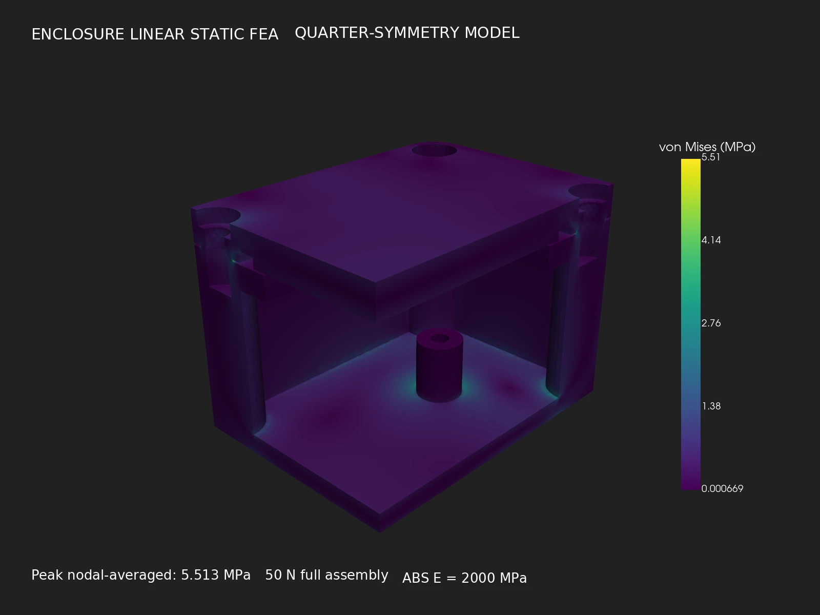
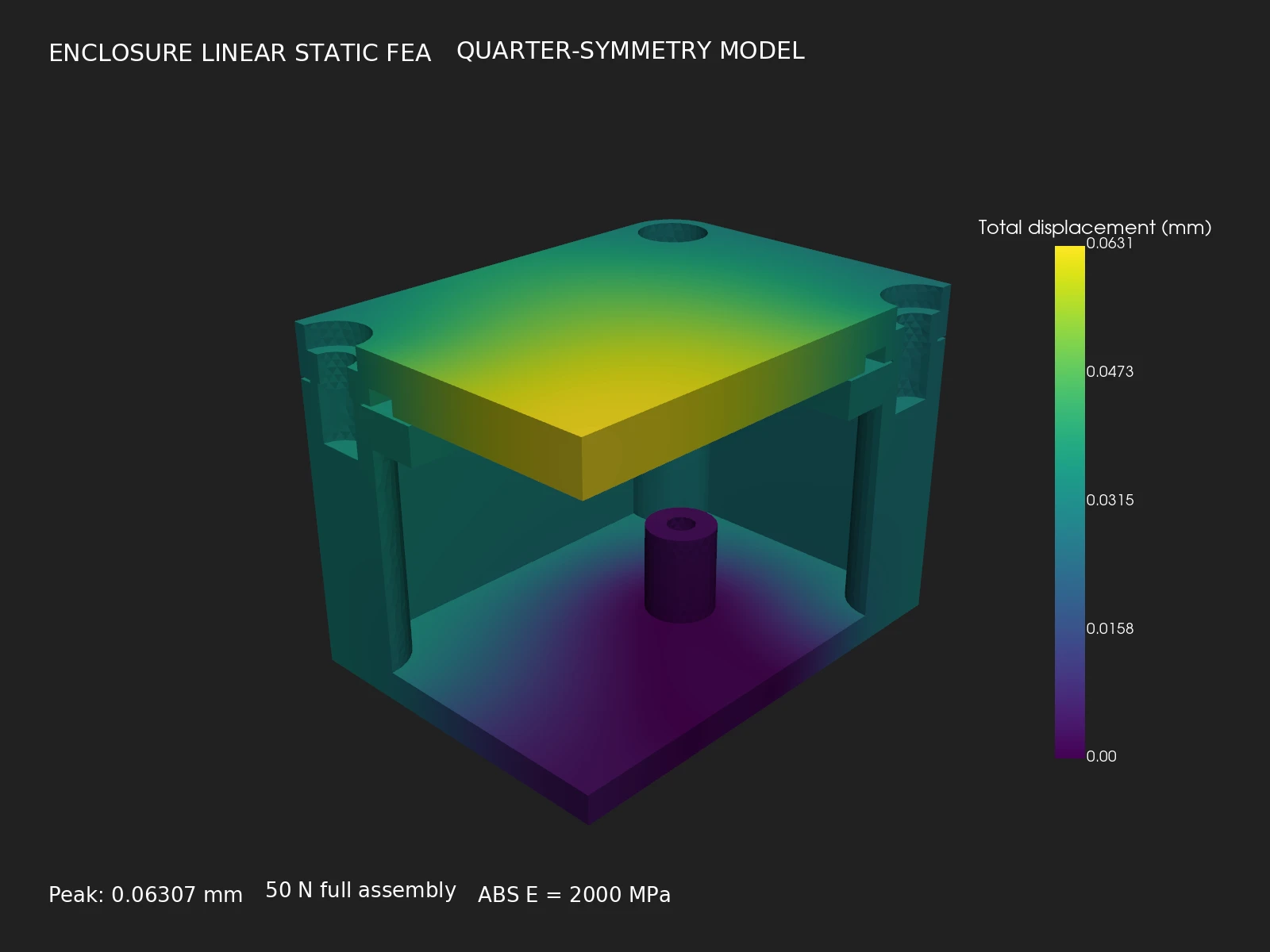
A separate ABS enclosure stress case used a 50 N lid load. It returned a peak nodal-averaged von Mises stress of 5.513 MPa and a maximum displacement of 0.063 mm. The sections below give the exact prompts, model setup, numerical checks, measured time, and Agent Compute Units.
1. Start with the board and enclosure
Keep the board envelope, mounting holes, regulator position, and housing in the same project. The original enclosure request was:
Create a simple sealed ABS electronics enclosure around a 50 x 30 mm PCB with four M3 mounting holes at 3.5 mm inset and a linear regulator dissipating 2 W at the center. Use a practical box, lid, mounting bosses, wall thickness, and sealed lid joint. Save the real 3D model in this project. Provide dimensions, downloadable model links, and a rendered image. Do not order anything or enter checkout.Flux produced a 25-solid STEP assembly with an approximately 76 × 56 × 27.4 mm envelope. This turn took 1,542.818 seconds and used 4.5 Agent Compute Units. Read Mechanical analysis for the analysis workflow.
2. Define one thermal design change
The thermal comparison uses an aluminum reconstruction of that enclosure. Both cases have the same PCB, regulator, bosses, lid, and small lid pedestal. The baseline leaves a 2 mm empty gap above the regulator. The comparison fills that gap with one thermal pad. This is the exact request:
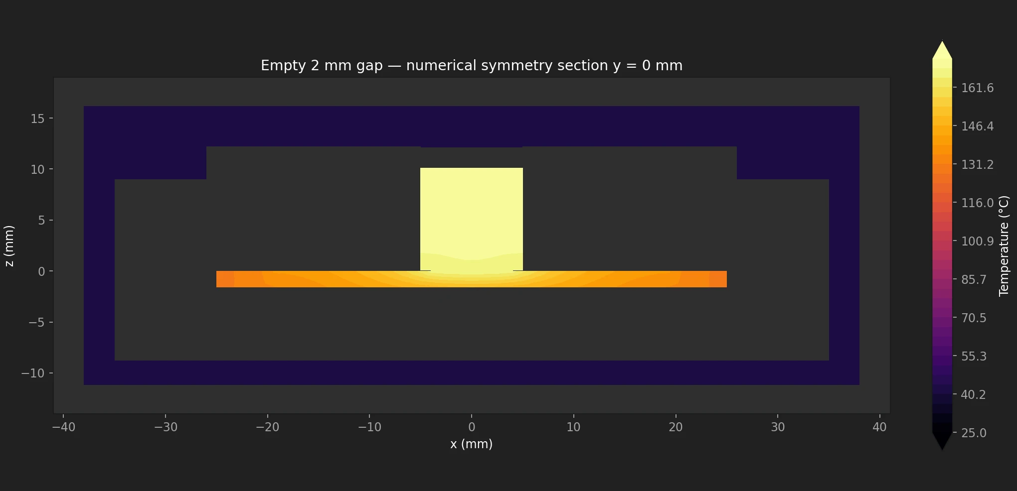
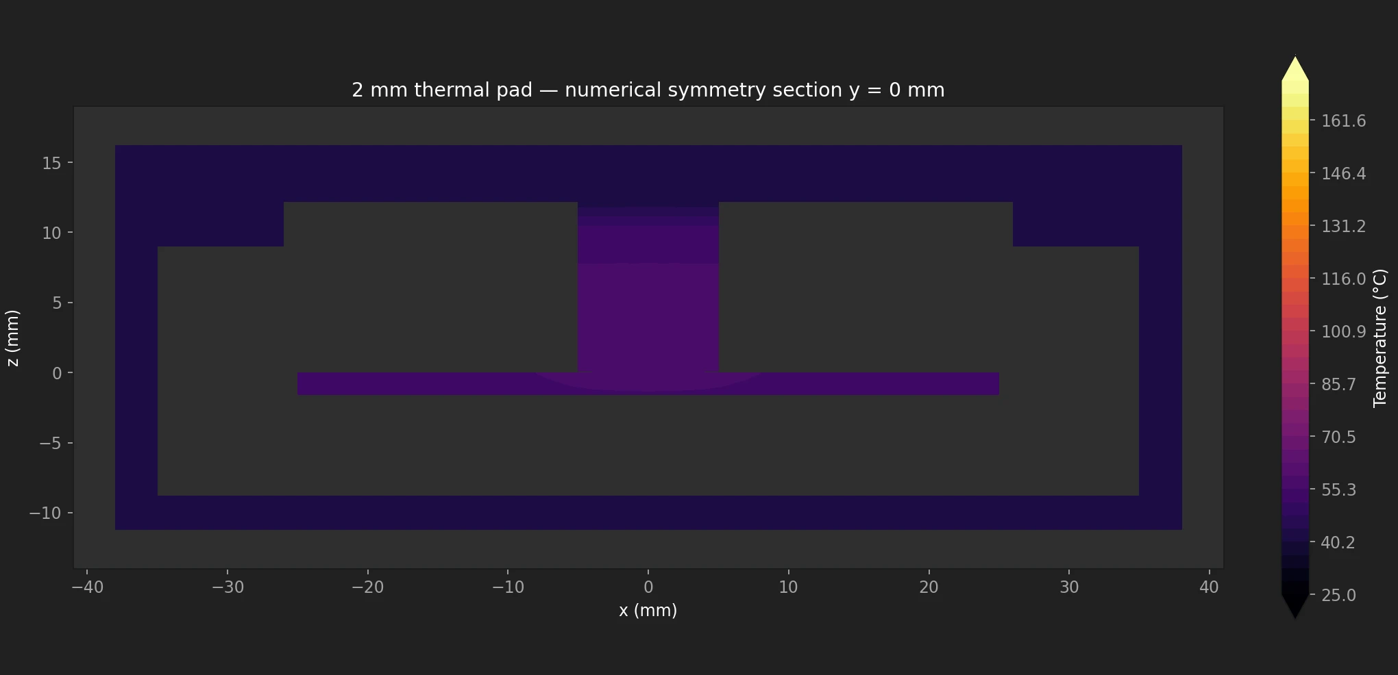
New conduction-only thermal pair; discard previous cavity models. Use this project's 50x30 mm PCB and 2 W regulator in an aluminum enclosure. Freeze both geometries/properties before solving: copper pours connect regulator to four mounting bosses; lid pedestal leaves a 2 mm gap above a 10x10 mm regulator pad face. Baseline: no thermal pad. Comparison: ONLY add a 2 mm thick, k=3 W/mK pad across that gap to the aluminum lid. All outer surfaces: h=8 W/m2K, ambient 25 C. All inner exposed surfaces adiabatic. NO air volume, internal convection, or radiation. State aluminum/PCB/copper properties and actual contact areas; ensure heat can leave through PCB/copper/bosses in baseline. Run both numerical steady solves, hand-check Rconv=1/(8*outer area) and Rpad=t/(k*A), report maximum/regulator mean C, integrated heat input/output and residual, mesh check, downloadable PNGs and numerical evidence. Do not tune to hit 40-120 C. At most these two solves; no retries. No orders or checkout.The frozen thermal setup
- Heat source: 2 W generated in a 10 × 10 × 10 mm regulator surrogate with conductivity 20 W/(m K). Reported regulator temperatures refer to this solid.
- Board: 50 × 30 × 1.6 mm, with two explicitly modeled 35 µm copper layers. Each connected copper pattern covers 70% of the usable board area. Copper conductivity is 385 W/(m K); FR4 conductivity is 0.30 W/(m K). The layers exchange heat through the 1.53 mm FR4 core.
- Regulator attachment: an 8 × 6 × 0.1 mm solder layer at 50 W/(m K) joins the regulator to the top copper.
- Enclosure: aluminum conductivity 167 W/(m K). Four bosses lie on the PCB hole axes, at (±21.5, ±11.5) mm. The annular board-to-boss contacts use 500 W/(m² K); their combined mesh area is 66.045 mm².
- Lid joint: an ideal bonded 0.2 mm gasket layer at 0.20 W/(m K), with 2,592 mm² per aluminum/gasket interface. The same joint appears in both cases.
- Pad: 10 × 10 × 2 mm, conductivity 3 W/(m K), with ideal full-face contact over 100 mm² at each end. A 10 × 10 × 0.1 mm lid projection leaves the 2 mm gap in both models.
- Cooling: 25 °C ambient and h = 8 W/(m² K) on all exterior faces, including the bottom. All inner exposed surfaces are adiabatic. The model has no air volume, internal convection, or radiation.
- Numerical setup: quarter symmetry, constant material properties, and one fixed mesh per case. The baseline has 12,555 nodes and 50,989 tetrahedra; the pad case has 12,601 nodes and 51,362 tetrahedra. The modeled copper pattern and lid projection are simulation geometry.
Without the pad, heat travels through solder, top copper, FR4, bottom copper, boss contacts, and the case. With the pad, a second path takes heat directly from the regulator to the lid.
3. Compare temperatures and heat flow
| Steady-state result | Empty gap | Thermal pad |
|---|---|---|
| Maximum temperature | 172.94 °C | 57.46 °C |
| Regulator volume mean | 171.24 °C | 56.27 °C |
| Heat generated | 2.000 W | 2.000 W |
| Exterior heat loss | 2.000 W | 2.000 W |
| Heat through boss contacts | 2.000 W | 0.263 W |
| Heat through the pad | 0 W | 1.737 W |
The pad reduced the maximum by 115.48 °C and the regulator volume mean by 114.97 °C. About 87% of the 2 W now leaves the regulator through the pad. The paired turn took 1,420.877 seconds and used 5.0 Agent Compute Units.
Hand-check the heat path
The tagged exterior area is 0.0157456 m². Its convection resistance is 1/(8 × 0.0157456) = 7.939 K/W. At 2 W, the area-weighted outer wall temperature is therefore approximately 25 + 2 × 7.939 = 40.88 °C.
The pad resistance is 0.002/(3 × 0.0001) = 6.667 K/W. At its solved 1.737 W heat flow, the pad drop is about 11.58 K. A regulator temperature above the roughly 41 °C wall, in the mid-50s, is consistent with that path. The finite boss contact alone contributes about 30.28 K/W to the baseline path.
An independent integration of the saved numerical fields reproduced both maxima and regulator volume means. It also reproduced the exterior area and 2 W source. Source-minus-exterior-loss residuals were −1.47 × 10⁻¹⁰ W for the baseline and +8.31 × 10⁻¹¹ W for the pad case.
4. Apply a lid load to the ABS enclosure
The stress example is a separate room-temperature, linear-elastic ABS reconstruction. It uses the original enclosure layout and a 50 N downward lid load. It is not a coupled calculation with the aluminum thermal pair.
Run a structural stress analysis of this enclosure with a total 50 N downward load distributed over the lid and the bottom mounting points fixed. State material properties, load and constraint assumptions. Report maximum von Mises stress in MPa and maximum displacement in mm. Provide a downloadable result image and identify whether this is an actual numerical simulation or an estimate. Do not order anything or enter checkout.- Material: homogeneous isotropic ABS, Young’s modulus E = 2,000 MPa and Poisson’s ratio ν = 0.35.
- Load: approximately 12.40 kPa uniform downward pressure over the exposed lid top, excluding screw holes, integrated to 50 N.
- Supports: four assumed circular underside patches of radius 2.8 mm, centered at (±21.5, ±11.5) mm. All three translations are fixed.
- Joint: eight ideal bonded lid-stop interfaces. The model uses quarter symmetry and quadratic tetrahedra.
| Mesh size | Peak nodal-averaged stress | Maximum displacement |
|---|---|---|
| 1.5 mm | 4.07 MPa | 0.06133 mm |
| 1.0 mm | 4.49 MPa | 0.06265 mm |
| 0.8 mm | 5.513 MPa | 0.06307 mm |
The finest mesh has 206,102 nodes and 128,504 elements. Maximum displacement is near the lid center. Peak stress is at an ideal bonded lid-stop edge. On the last refinement, displacement changed by 0.68% and the peak stress changed by 22.7%. The full-model vertical support reaction is 50.00036 N for the 50 N load.
This numerical stress turn took 1,547.959 seconds and used 3.3 Agent Compute Units.
When to move to Ansys or SimScale
Move to Ansys or SimScale when the design question requires transient heating, convection-heavy airflow, opening or sliding contact, or a certification workflow. Carry the geometry, source power, material properties, support definitions, and result fields into that next study. Keep the electronics and enclosure assumptions together so the next analysis answers the same design question.
For a circuit example, read Simulate circuits with a prompt. For the setup process, read Hardware simulation with scoped approximations and the simulation reference.
FAQs
State the PCB dimensions, enclosure material, heat source or mechanical load, and boundary conditions. Ask for the numerical result, result images, material properties, and balance checks. Keep the setup with the board and enclosure in the same project.
The comparison adds one 10 × 10 × 2 mm thermal pad from the regulator to the aluminum lid. Both cases use 2 W, 25 °C ambient, and exterior convection of 8 W/(m² K). The regulator maximum changed from 172.94 °C to 57.46 °C.
A 50 N downward load was distributed over the lid. Four underside patches were fixed in all three translations. With ABS E = 2,000 MPa and ν = 0.35, the finest mesh returned 5.513 MPa peak nodal-averaged stress and about 0.063 mm maximum displacement.
The paired thermal turn used 5.0 Agent Compute Units and took 1,420.877 seconds. The separate stress turn used 3.3 Agent Compute Units and took 1,547.959 seconds. The original enclosure creation used 4.5 Agent Compute Units.
More in PCB Design & Engineering Fundamentals

What Is a PCB? A Beginner's Guide to Printed Circuit Board Design

What is Schematic Design? All You Need to Know

PCB Stackup Design: How to Build the Right Layer Structure

Best PCB Routing Techniques for Clean Circuit Board Layouts

How to Read PCB Schematics: A Beginner-Friendly Guide

PCB Schematic Best Practices for Clean Circuit Design

Schematic Capture Explained: How Engineers Create Circuit Diagrams

What Is EDA Software? A 2026 Guide to Tools and Companies

Best Schematic Capture Software in 2026: 7 Tools Compared

Common Schematic Design Mistakes and How to Avoid Them

PCB Netlists Explained: How Schematics Connect to Layouts

What Is a Netlist? Understanding the Basics of Electronic Design Automation

PCB Symbol Design: Best Practices for Clean Schematics

Making Parts Just Got Easier: Introducing Parametric Symbols

Create Satisfying Schematics with these Updates

Electronic Circuit Design Explained: From Schematics to PCB Layout

Designing PCBs: What Are the Essential Steps

Hardware Design Workflow: From Schematic Capture to Manufacturing

What Is a Functional Block Diagram and Why Is It Critical in System Design

PCB Design Basics: What You Need to Know Before You Start

Diode Symbols: How to Identify Common Diodes

Ultra Librarian joins Flux to Take the Hard out of Hardware

Flux Now Has the World's Largest eCAD Part Library

Capacitor Symbols Explained: Types, Polarity, and Schematic Use

MOSFET and Transistor Symbols Explained: NMOS, PMOS, NPN, and PNP

How to Convert PDF Schematics into Editable EDA Files Using AI

Resistor Symbols Explained: Fixed, Variable, Thermistor, and Photoresistor Symbols

Fuse Symbols Explained: Electrical, Thermal, and Circuit Protection Symbols

How to Learn PCB Design: A Step-by-Step Roadmap for Beginners

Crosstalk, Reflections, and the Real Challenges of Signal Integrity

What Is Signal Integrity in PCB Design? A Practical Guide

High-Speed PCB Design: Layout Rules, Signal Integrity, and Routing Best Practices

EMI/EMC in PCB Design: How to Reduce Interference

PCB EMI Problems: Causes and Solutions

Differential Pair Routing Guidelines and Controlled Impedance Best Practices

PCB Impedance Control: A Practical Guide for Engineers

Introducing Curved Traces in Flux

Analog vs Digital PCB Design: Key Differences Explained

Pi Filters Explained: Design, Components & Applications

RS485 Explained: Wiring, Specifications, and Applications

What is RS232?

SPI vs. I2C: Which Communication Protocol Should You Use?

RJ45 Connectors: Pinouts, Categories, Uses, and Testing

CO2 Sensor Technology: How These Devices Detect Carbon Dioxide

Hall Effect Joysticks: How They Work, Benefits, and Uses

What Is an Oscillator? Beginner's Guide to Oscillating Circuits

Flexible PCB Design Guide: Materials, Layout, and Applications

Rigid-Flex PCB Design: Benefits, Challenges, and Layout Tips

The RF Engineer's Guide to Designing Printed Trace Antennas

SMA Connectors Explained: Types, Applications, and PCB Design Considerations

RC Low-Pass Filter: Formula, Cutoff Frequency & Design

NFC vs RFID: Board Design, Tags, and Reader Choices

Low-Pass vs High-Pass Filter: Differences and Examples

How to Choose a Bluetooth Module for Your PCB Design

Decoding Voltage Regulators: How They Work in Everyday Electronics

Voltage Regulators: How They Work, Types, and Applications

Buck Converter Design: Components, PCB Layout, and Formulas

Buck and Boost Converters: How They Work and Where They’re Used

LM2596 in Action: Case Study of Its Application in Power Supply Units

Guide to GND Fills and Power Planes

Power Distribution Network (PDN) Design in PCBs

PCB Grounding Techniques for Noise Reduction and Stability

Designing High-Current PCBs: Layout and Safety Considerations

How to Calculate PCB Trace Resistance

Voltage Drop Calculations: Formulas, Factors, and Guidelines

AC to DC Converter: The Backbone of Power Electronics

AC-to-DC Converters: How They Work, Types, and Design Tips

Thermal Management in PCB Design: Methods and Best Practices

PCB Thermal Management: Analysis and Design Best Practices

Understanding PPS Fast Charging: What It Is and How It Works

Decoupling Capacitors in PCB Design: Placement and Selection

What Is a Multilayer Ceramic Capacitor (MLCC)?

Tantalum Capacitors Guide: Polarity, Derating & Risks

Amps vs. Volts: Key Differences and How They Work Together

Current Sensor Types: Shunt, Hall Effect, and Current Transformer Comparison

Li-ion vs LiPo vs LiFePO4 vs NiMH for Hardware Design

Never Worry About Stackups Again: Introducing the Stackup Editor

Multilayer PCB Design: Stackup and Routing Best Practices

How to Choose PCB Materials: FR4 vs Advanced Substrates

Blind Vias, Buried Vias, and Microvias: A Complete Guide to PCB Via Types

Exploring Different Types of Vias in PCB

High-Density PCBs just got easier with Smart Vias

How to Use Via Stitching in PCB Design

PCB Design Constraints: What Engineers Need to Know

PCB Constraint Management: How Engineers Control Layout Rules

Design Rule Checking (DRC) in PCB Design: Real-Time vs Batch, Rules, and Common Failures

Electrical Rule Check (ERC) vs DRC in PCB Design

PCB Design Reviews: Best Practices for Catching Errors Early

Common PCB Design Mistakes and How to Avoid Them

5 Common PCB Design Mistakes and How to Avoid Them

PCB Silkscreen Design: Guidelines and Common Mistakes

Smart Polygons: Advanced PCB Design Just Got Easier

Automatically Create Photorealistic PCB Renders

How to Convert from MM to Mils: a Guide for Beginners

What Is Solder Mask? Materials, Colors, and PCB Design Rules

Designing Custom PCB Outlines: Fixing DXF and SVG Import Failures

PCB Enclosure Design: How to Design an Enclosure

How to design a sheet metal bracket for your PCB with a text prompt

Designing hinges, snap-fits and moving parts for your enclosure in Flux

PCB IPC Standards Explained: IPC-2221, IPC-2152, IPC-7351, and More

Component Selection in PCB Design: How Engineers Choose the Right Parts

Smarter Part Search Just Got a Major Upgrade

How to Design a PCB Footprint (Step-by-Step Guide)

Protection Circuit 101: Securing Your Electronics from Overcurrent and Short Circuits

Understanding the Flyback Diode: Your Essential Guide to Functionality and Why You Need One

What Is a Zener Diode? How It Works and Where It’s Used

Understanding the Fundamentals: MOSFET Basics for Beginners

NMOS vs PMOS: Differences & When to Use Each

NPN vs PNP Transistors: Differences & When to Use Each

LM741 Pinout: A Deep Dive into a Classic Op Amp

6 Types of Variable Resistors: a Detailed Look at Their Uses
Parallel and Series Resistor Calculator

Resistor Color Code Calculator

SMT vs Through-Hole Technology: Which Should You Use?

How to Use Flux When Soldering Electronics

The Ultimate Guide to Toggle Switches: Types, Uses, and How They Work

What Is the Science Behind Push Button Switches and How They Work

Tactile Switches: Wiring, Debouncing, and PCB Design

Electrical Wire Connector Types and Uses

Board-to-Board Connectors: Types, Pitch and Stack Height

RTD vs Thermocouple vs Thermistor: Sensor Selection

Why Your PCB Is Failing: Debugging Common Issues

555 Timer Guide: Pinout, Operating Modes, and Circuit Examples

Inverting Op-Amp Circuits: Formula, Gain, and Design Examples

How to Wire a Potentiometer: Pinout, Diagrams, and PCB Examples
Let’s start building.

Let’s build your idea together. All you need to do is describe what you want to make, or what problem you want to solve. Flux will work with you to make it a reality.
