


Designing hinges, snap-fits and moving parts for your enclosure in Flux

Flux is an AI hardware engineer that designs the electronics and mechanical parts of a device in one project. For a moving enclosure, start with the board, choose a hinge or snap-fit mechanism, and specify the mating geometry. This walkthrough uses a removable-pin hinge around a real 72 × 100 mm ESP32 computer board.
The result is a PETG base and lid, a five-knuckle hinge, a removable pin, and closed and open assemblies. Independent measurements of the exported files reproduced the 3.0 mm pin, 3.4 mm bores, four 0.3 mm axial gaps, and 1.0 mm board-side clearance. The two requests took about 82 minutes of recorded processing time and used 53.4 Agent Compute Units.
1. Start from an editable fork of the board
Open the public ESP32 x86 PC project. Use the project action menu to select Fork Project, then choose your workspace. Work in that fork so the PCB and its component models belong to the same project as the enclosure.
This board includes USB, VGA, PS/2, and card connectors. Its native 3D export measures 72 × 100 × 1.29936 mm. Four 2.2 mm mounting holes sit at layout coordinates (±33, ±47) mm. Those features define the support positions, connector openings, and enclosure envelope.
The first request specifies the mechanism, fit, motion, and files together:
Design a PETG enclosure with a working pin-hinged lid around THIS project's actual PCB. This is an editable fork of vasy_skral/esp32-x86-pc; use the CURRENT project's native board 3D export, not a guessed rectangle or cross-project export. Read board, components, connectors and mounting holes. Keep electronics unchanged. Use 1 mm side clearance, 2 mm component headroom, 3 mm removable pin, 3.4 mm hinge bores and 0.3 mm axial gaps. Check closed fit and 0-110 degree opening for interference with board, case and pin; report measured clearances and failures. Produce named closed/open STEP assemblies with actual PCB, separate watertight printable base/lid STLs, pin STEP, source, fit report and PNG renders closed/open/exploded. State print orientation and tolerances; verify board retention and assembly paths. If actual PCB export or a functional hinge is blocked, stop and report; do not substitute a decorative hinge. No orders, checkout, payments or external messages.Read Make mechanical parts for the mechanical design workflow. Keeping the actual board in the project lets the enclosure use its connector positions and component heights.
2. Inspect connector orientation without changing the electronics
Connector orientation determines both the opening and the direction in which a cable enters. Give Flux permission to inspect the footprint and manufacturer drawing before it changes a component model. This run used the following exact follow-up:
Yes, correct USB1's 3D-model transform in THIS fork if its footprint and manufacturer drawing show it is wrong. Verify mounting orientation first. Keep footprint, PCB placement, parts, nets and connections unchanged. Then continue straight to a functional PETG enclosure with a hinged or snap-fit lid around the actual PCB and connectors. Retain 1 mm side clearance, 2 mm component headroom, and, for a hinge, a 3 mm removable pin, 3.4 mm bores and 0.3 mm axial gaps. Check PCB/connector fit, retention, connector mating paths, assembly and 0-110 degree opening for interference. Deliver measured tolerances/clearances, named closed/open STEP assemblies, separate watertight printable STLs, editable source and closed/open/exploded PNG renders in this fork. Proceed through design and verification without another checkpoint for these authorized choices. No orders, checkout, payments or external messages.The inspection supported USB1's existing upright side-mount orientation, so Flux kept its transform. The enclosure design used the existing PCB, hole positions, and component models. The closed assembly retained the 91 modeled electronic entries from the board reference.
3. Specify pin, bore, and knuckle clearances
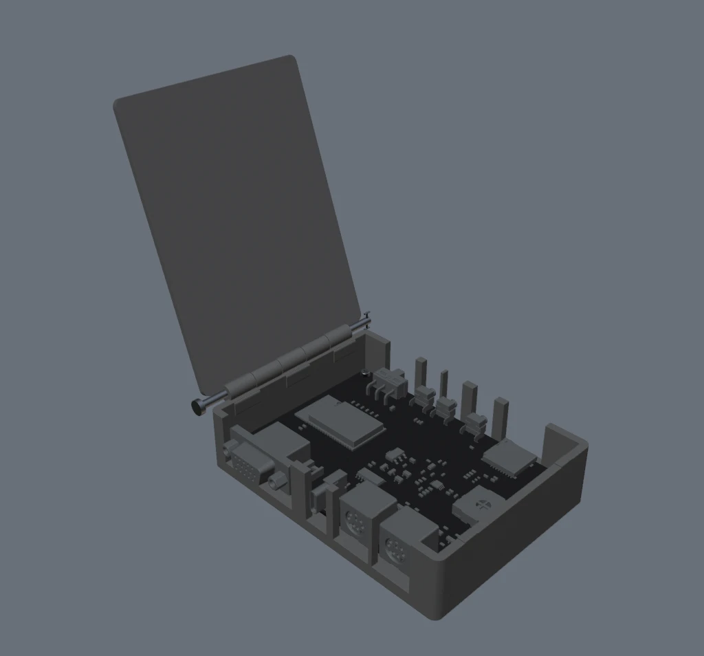
The hinge alternates three base knuckles with two lid knuckles. A removable pin runs through their common axis. The main case outline is 80 × 108 mm before the hinge projection. Ordinary walls are 3.0 mm thick; the floor and lid plate are each 2.4 mm thick.
| Nominal CAD feature | Measured value |
|---|---|
| Pin diameter | 3.000 mm |
| Hinge bore diameter | 3.400 mm |
| Diametral clearance | 0.400 mm |
| Radial clearance | 0.200 mm |
| Axial gaps between adjacent knuckles | Four gaps, 0.300 mm each |
| Closed lid seating | Gravity-seated on seating lands |
These dimensions define the CAD fit. Keep radial clearance separate from diametral clearance: the difference between the bore and pin diameters is 0.4 mm, while the space on each side of a centered pin is 0.2 mm. Use the nominal geometry to set the print process and bore calibration.

4. Check the board, components, and lid motion
Independent checks imported the final native STEP and measured the enclosure against the PCB and component solids. The measured fit was:
| Fit check | Measured value |
|---|---|
| Ordinary PCB side clearance | 1.000 mm on each side |
| Headroom above the highest modeled component | 2.800 mm |
| Clearance below the lowest modeled component | 3.200 mm |
| Minimum base-to-component clearance | 0.895 mm |
| Unintended base/PCB volumetric overlap | 0 mm³ |
The enclosure retains the board with four screws and inserts. Its cutouts follow the modeled connectors. The fit report also records provisional cable access envelopes and assembly paths. Use Fit and clearance to define the specific mating parts and access spaces for your device.
The independent motion check sampled 111 poses from 0° through 110° at 1° intervals. It checked the lid against the base, PCB, a component envelope, pin, and retainer. None of those samples had unintended overlap above the 0.001 mm³ check threshold. The exported open assembly's lid plane measured 110.000° relative to its closed pose.
5. Export the shells, pin, and assemblies
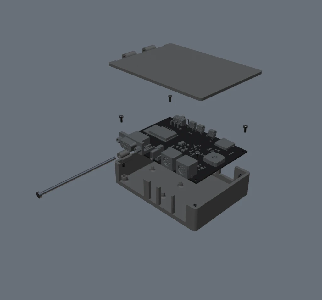
Flux produced separate printable base and lid meshes, a pin solid, editable source, and named assemblies containing the actual board. Independent mesh checks found both STLs watertight, consistently wound, and connected as one body each.
- Base STL: 85,890 triangles, oriented floor-down.
- Lid STL: 2,620 triangles, oriented edge-down with the hinge axis vertical.
- Pin STEP: a separate solid for the removable pin.
- Closed STEP archive and 110° open STEP archive: named solid assemblies.
- Editable source pack and measured fit report.
Use the STLs for the PETG print workflow. Extract the STEP archives to carry named solid geometry into downstream CAD or CAM. See Mechanical drawings and exports for the file workflow.
Recorded time and Agent Compute Units
The run starts with the editable fork and includes both exact requests above. Wall time measures each request through its final result. Agent Compute Units measure the reported compute use; work within each request is included in that total.
| Request | Wall time | Agent Compute Units |
|---|---|---|
| Board inspection and enclosure request | 840.335 seconds | 2.5 |
| Model inspection, hinge design, and verification | 4,087.315 seconds | 50.9 |
| Total recorded processing time | 4,927.650 seconds | 53.4 |
For a complementary fabrication example, follow the sheet-metal bracket walkthrough. For enclosure loads and heat paths, read the thermal and stress simulation walkthrough.
FAQs
Work in an editable project that contains the PCB and its component models. Specify the enclosure material, board clearances, hinge geometry, opening angle, and export files. This example starts from a fork of a 72 × 100 mm ESP32 computer board.
The nominal CAD pin diameter is 3.0 mm and the bore diameter is 3.4 mm. That gives 0.4 mm diametral clearance and 0.2 mm radial clearance. Four axial gaps between adjacent knuckles measure 0.3 mm each.
Independent geometry checks sampled 111 lid poses at 1° intervals from 0° through 110°. The checks included the base, PCB, component envelope, pin, and retainer. No sampled pose had unintended overlap above 0.001 mm³.
Flux produced separate watertight base and lid STLs, a pin STEP, and named closed and open STEP assemblies in compressed archives. It also produced editable source, a measured fit report, and closed, open, and exploded PNG renders. The STLs include print orientations for the PETG shells.
More in PCB Design & Engineering Fundamentals

What Is a PCB? A Beginner's Guide to Printed Circuit Board Design

What is Schematic Design? All You Need to Know

PCB Stackup Design: How to Build the Right Layer Structure

Best PCB Routing Techniques for Clean Circuit Board Layouts

How to Read PCB Schematics: A Beginner-Friendly Guide

PCB Schematic Best Practices for Clean Circuit Design

Schematic Capture Explained: How Engineers Create Circuit Diagrams

What Is EDA Software? A 2026 Guide to Tools and Companies

Best Schematic Capture Software in 2026: 7 Tools Compared

Common Schematic Design Mistakes and How to Avoid Them

PCB Netlists Explained: How Schematics Connect to Layouts

What Is a Netlist? Understanding the Basics of Electronic Design Automation

PCB Symbol Design: Best Practices for Clean Schematics

Making Parts Just Got Easier: Introducing Parametric Symbols

Create Satisfying Schematics with these Updates

Electronic Circuit Design Explained: From Schematics to PCB Layout

Designing PCBs: What Are the Essential Steps

Hardware Design Workflow: From Schematic Capture to Manufacturing

What Is a Functional Block Diagram and Why Is It Critical in System Design

PCB Design Basics: What You Need to Know Before You Start

Diode Symbols: How to Identify Common Diodes

Ultra Librarian joins Flux to Take the Hard out of Hardware

Flux Now Has the World's Largest eCAD Part Library

Capacitor Symbols Explained: Types, Polarity, and Schematic Use

MOSFET and Transistor Symbols Explained: NMOS, PMOS, NPN, and PNP

How to Convert PDF Schematics into Editable EDA Files Using AI

Resistor Symbols Explained: Fixed, Variable, Thermistor, and Photoresistor Symbols

Fuse Symbols Explained: Electrical, Thermal, and Circuit Protection Symbols

How to Learn PCB Design: A Step-by-Step Roadmap for Beginners

Crosstalk, Reflections, and the Real Challenges of Signal Integrity

What Is Signal Integrity in PCB Design? A Practical Guide

High-Speed PCB Design: Layout Rules, Signal Integrity, and Routing Best Practices

EMI/EMC in PCB Design: How to Reduce Interference

PCB EMI Problems: Causes and Solutions

Differential Pair Routing Guidelines and Controlled Impedance Best Practices

PCB Impedance Control: A Practical Guide for Engineers

Introducing Curved Traces in Flux

Analog vs Digital PCB Design: Key Differences Explained

Pi Filters Explained: Design, Components & Applications

RS485 Explained: Wiring, Specifications, and Applications

What is RS232?

SPI vs. I2C: Which Communication Protocol Should You Use?

RJ45 Connectors: Pinouts, Categories, Uses, and Testing

CO2 Sensor Technology: How These Devices Detect Carbon Dioxide

Hall Effect Joysticks: How They Work, Benefits, and Uses

What Is an Oscillator? Beginner's Guide to Oscillating Circuits

Flexible PCB Design Guide: Materials, Layout, and Applications

Rigid-Flex PCB Design: Benefits, Challenges, and Layout Tips

The RF Engineer's Guide to Designing Printed Trace Antennas

SMA Connectors Explained: Types, Applications, and PCB Design Considerations

RC Low-Pass Filter: Formula, Cutoff Frequency & Design

NFC vs RFID: Board Design, Tags, and Reader Choices

Low-Pass vs High-Pass Filter: Differences and Examples

How to Choose a Bluetooth Module for Your PCB Design

Decoding Voltage Regulators: How They Work in Everyday Electronics

Voltage Regulators: How They Work, Types, and Applications

Buck Converter Design: Components, PCB Layout, and Formulas

Buck and Boost Converters: How They Work and Where They’re Used

LM2596 in Action: Case Study of Its Application in Power Supply Units

Guide to GND Fills and Power Planes

Power Distribution Network (PDN) Design in PCBs

PCB Grounding Techniques for Noise Reduction and Stability

Designing High-Current PCBs: Layout and Safety Considerations

How to Calculate PCB Trace Resistance

Voltage Drop Calculations: Formulas, Factors, and Guidelines

AC to DC Converter: The Backbone of Power Electronics

AC-to-DC Converters: How They Work, Types, and Design Tips

Thermal Management in PCB Design: Methods and Best Practices

PCB Thermal Management: Analysis and Design Best Practices

Understanding PPS Fast Charging: What It Is and How It Works

Decoupling Capacitors in PCB Design: Placement and Selection

What Is a Multilayer Ceramic Capacitor (MLCC)?

Tantalum Capacitors Guide: Polarity, Derating & Risks

Amps vs. Volts: Key Differences and How They Work Together

Current Sensor Types: Shunt, Hall Effect, and Current Transformer Comparison

Li-ion vs LiPo vs LiFePO4 vs NiMH for Hardware Design

Never Worry About Stackups Again: Introducing the Stackup Editor

Multilayer PCB Design: Stackup and Routing Best Practices

How to Choose PCB Materials: FR4 vs Advanced Substrates

Blind Vias, Buried Vias, and Microvias: A Complete Guide to PCB Via Types

Exploring Different Types of Vias in PCB

High-Density PCBs just got easier with Smart Vias

How to Use Via Stitching in PCB Design

PCB Design Constraints: What Engineers Need to Know

PCB Constraint Management: How Engineers Control Layout Rules

Design Rule Checking (DRC) in PCB Design: Real-Time vs Batch, Rules, and Common Failures

Electrical Rule Check (ERC) vs DRC in PCB Design

PCB Design Reviews: Best Practices for Catching Errors Early

Common PCB Design Mistakes and How to Avoid Them

5 Common PCB Design Mistakes and How to Avoid Them

PCB Silkscreen Design: Guidelines and Common Mistakes

Smart Polygons: Advanced PCB Design Just Got Easier

Automatically Create Photorealistic PCB Renders

How to Convert from MM to Mils: a Guide for Beginners
What Is Solder Mask? Materials, Colors, and PCB Design Rules

Designing Custom PCB Outlines: Fixing DXF and SVG Import Failures

PCB Enclosure Design: How to Design an Enclosure

How to design a sheet metal bracket for your PCB with a text prompt

How to run thermal and stress simulation on a PCB enclosure in the browser

PCB IPC Standards Explained: IPC-2221, IPC-2152, IPC-7351, and More

Component Selection in PCB Design: How Engineers Choose the Right Parts

Smarter Part Search Just Got a Major Upgrade

How to Design a PCB Footprint (Step-by-Step Guide)

Protection Circuit 101: Securing Your Electronics from Overcurrent and Short Circuits

Understanding the Flyback Diode: Your Essential Guide to Functionality and Why You Need One

What Is a Zener Diode? How It Works and Where It’s Used

Understanding the Fundamentals: MOSFET Basics for Beginners

NMOS vs PMOS: Differences & When to Use Each

NPN vs PNP Transistors: Differences & When to Use Each

LM741 Pinout: A Deep Dive into a Classic Op Amp

6 Types of Variable Resistors: a Detailed Look at Their Uses
Parallel and Series Resistor Calculator

Resistor Color Code Calculator

SMT vs Through-Hole Technology: Which Should You Use?

How to Use Flux When Soldering Electronics

The Ultimate Guide to Toggle Switches: Types, Uses, and How They Work

What Is the Science Behind Push Button Switches and How They Work

Tactile Switches: Wiring, Debouncing, and PCB Design

Electrical Wire Connector Types and Uses

Board-to-Board Connectors: Types, Pitch and Stack Height

RTD vs Thermocouple vs Thermistor: Sensor Selection

Why Your PCB Is Failing: Debugging Common Issues

555 Timer Guide: Pinout, Operating Modes, and Circuit Examples

Inverting Op-Amp Circuits: Formula, Gain, and Design Examples

How to Wire a Potentiometer: Pinout, Diagrams, and PCB Examples
Let’s start building.

Let’s build your idea together. All you need to do is describe what you want to make, or what problem you want to solve. Flux will work with you to make it a reality.
