


Flex and Rigid-Flex Boards Are in Flux

Most real devices bend somewhere.
An earbud folds its board around the battery. A smartwatch wraps its sensors around the case. A camera module sends its image data down a thin flex tail to the main board.
Today the Flux agent designs those boards too. Flux now designs pure-flex and rigid-flex boards, from the stackup to the manufacturing files.
A camera for a pair of smart glasses
Here is a scenario. Dana is a hardware engineer on a smart-glasses team. The camera must sit in the front of the frame, next to the hinge. Its image data must go 40 mm along the temple arm to the main board. The sensor board can be 10 × 10 mm at most, and the lens can be 6 mm high at most.
Dana opens a Flux project and gives the requirement to the agent:
Design a 5 MP camera module for a pair of smart glasses. Use a 4-layer rigid board for the image sensor and a 2-layer flex tail, 40 mm long, to a board-to-board connector on the main board. Add a stiffener under the connector.
The agent first asks which camera input the main board has and how much space the module gets. Dana answers: a 2-lane MIPI CSI-2 input on the application processor, and the size limits. The agent writes the requirements into a project specification. It selects a 5 MP image sensor and a board-to-board connector, captures the circuit, and reviews the circuit and fixes what the review finds.
Then the agent sets up the board. It makes a 4-layer rigid area stackup for the 10 × 10 mm sensor board and a 2-layer flex area stackup for the 40 mm tail. The two flex copper layers are the inner layers of the rigid board, so they continue from the sensor board into the tail. The agent adds a 0.4 mm FR-4 stiffener under the connector.
In about one hour, Dana has a specification, a selected sensor and connector, a reviewed circuit, and the area stackups for the rigid board and the flex tail, with a stiffener under the connector.
Next, Dana asks the agent to fold the tail 90° at the hinge. The 3D view shows the folded tail in the frame of the glasses.
What Flux does on a flex or rigid-flex board
You give the agent the requirement. The agent sets up the stackups, draws the areas, places, routes, checks and exports. You can also do each step yourself in the editor.
| Area | What Flux does |
|---|---|
| Stackups | The board has one layer stack. Named area stackups, of the kind Rigid or Flex, select layers from it, so a copper layer keeps its name and number in each area. One area stackup is the default for the rest of the board. Each area stackup shows its thickness and its number of copper layers. |
| Templates | Flex 2 Layer, Rigid-Flex 4 Layer, JLCPCB Flex 1 Layer, JLCPCB Flex 2 Layer, JLCPCB Flex 4 Layer with electro-deposited copper, and JLCPCB Flex 4 Layer with bend-rated rolled annealed copper. |
| Materials and layers | Polyimide, polyimide + adhesive, bondply, rolled annealed copper and electro-deposited copper. Coverlay layers, stiffener layers and shield film. |
| Stackup Areas | The agent draws, renames and assigns the Stackup Areas. The canvas shows each area with its name and its area stackup. |
| Parts on flex areas | A part on a flex area sits on the outer copper layer of that area. Its pads open the coverlay. |
| Routing | Each net goes only on the layers of the area that it crosses. No vias where the area stackup does not allow them. Impedance-controlled trace widths come from the stackup of the area. |
| Copper pours | Pours in flex areas are hatched: 0.25 mm lines, 0.5 mm gap, 45°, a 0.5 mm solid border, and solid rings around pads and vias of the same net. Rigid areas keep solid pours. |
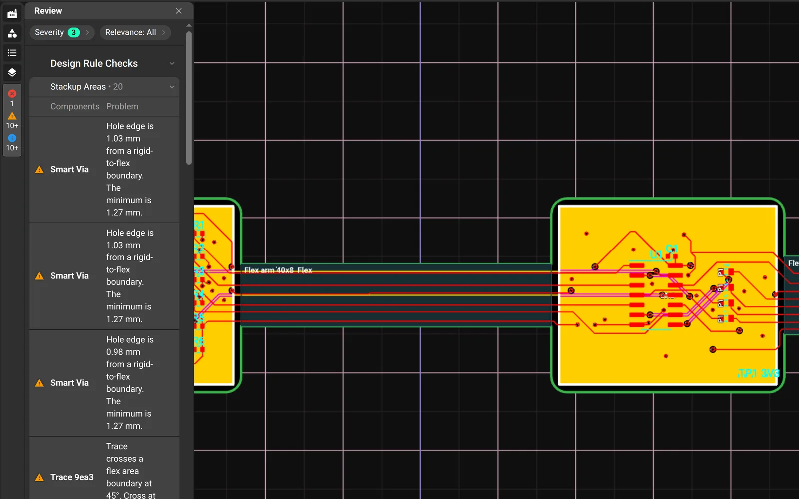
| Flex design checks | Parts on bare flex without a stiffener. Pads too near a stiffener edge. Vias and plated holes in bare flex. Holes and pads too near a rigid-to-flex boundary. Traces that cross a rigid-to-flex boundary at an angle other than 90°. Trace corners and width changes near a boundary. Traces stacked on adjacent flex layers. Sharp trace corners in bare flex. Solid copper pours in a flex area. Copper too near the board edge. Pads and vias without teardrops. Coverlay openings too small for the pad. Flex area stackups without coverlay on an outer copper layer. Bend radius information for each flex area. Stackup Areas with an unknown area stackup. |
| Signal checks | Impedance, crosstalk, electrical length, differential pairs, vias and DC resistance use the stackup of each area. |
| Simulation | Electromagnetic and thermal simulations use the stackup of each Stackup Area. |
| 3D | Each area shows at its own thickness, with coverlay and stiffeners. 3D downloads in STEP, compressed STEP, BREP, XAO, GLB, STL, OBJ and COLLADA. |
| Bends and twists | Add a Flex Joint to a flex Stackup Area, or to the board on a pure-flex board. Its Bend rule, for example 90deg 1mm, sets the bend angle and the bend radius. Its Twist rule, for example 90deg 20mm, sets the twist angle and the twist length. Set one or both. A Flex Joint also has Position, Rotation and Repeated Bending rules. The agent adds and edits Flex Joints from chat. Flux shows each bend zone, shows the folded board in the 3D view and folds the 3D downloads. Design checks: bend radius against the minimum for the flex stackup, which is larger for repeated bending; minimum twist length for the width of the tail; no parts, pads, vias or holes in a bend or twist zone; traces at 90° across a bend; and zones that overlap. Altium projects import with their bend lines. |
| Enclosure fit in 3D | Put the folded board in the enclosure in the 3D assembly and check the clearance. Change the bends until the board fits. |
| Manufacturing files | Gerber files for each coverlay layer, each stiffener layer and the Stackup Area outlines. A fabrication drawing PDF with the area stackup, finished thickness and size of each area. A stackup area list. IPC-2581C and ODB++ with one stackup for each area stackup. |
| Imports | IPC-2581 and ODB++ boards open with their rigid and flex area stackups, Stackup Areas and coverlay layers. |
| Quotes and orders | JLCPCB quotes and makes flex boards. The order uses the construction of the quote that you approved. PCBWay quotes flex and rigid-flex boards. |
| Saved boards | A saved flex or rigid-flex board opens with its Stackup Areas, 3D view, design checks and exports for every person who opens the project. |
One board. A stackup for each area.
A rigid-flex board does not have one stackup. It has a rigid stackup in some areas and a thin flex stackup in other areas.
In Flux, you draw Stackup Areas on the board. Each area gets a named stackup, for example "Rigid 4 layer" for the sensor board and "Flex 2 layer" for the tail. All of these stackups come from one layer list. A copper layer keeps its identity when it goes from a rigid area into a flex area. A trace on the second copper layer of the rigid board is still on that layer in the flex.
The flex materials are in the stackup editor: polyimide, polyimide with adhesive, bondply, coverlay, rolled annealed and electro-deposited copper, stiffeners and shield film. Start from the Flex 2 Layer or Rigid-Flex 4 Layer template, or from a JLCPCB Flex template with 1, 2 or 4 layers.
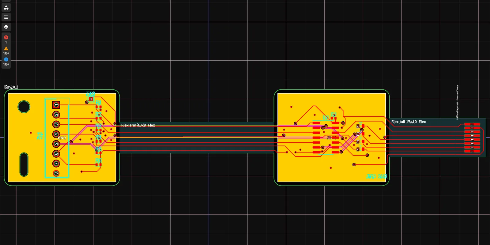
The agent knows which area it works in
Routing, copper pours, vias, placement, design checks, impedance and simulation all follow the stackup of each area.
Route a differential pair from the rigid board into the flex tail. Impedance, crosstalk and delay for that pair use the flex dielectric in the tail and the rigid core on the board. Auto-routing stays inside the limits of each area. Copper pours in flex areas are hatched, so the tail stays flexible. Simulation uses the real layers and thicknesses of each area.
The design checks know flex. Flux checks the bend radius, coverlay openings, outer copper without coverlay, holes, vias and parts in flex areas without a stiffener, pads and holes too near a rigid-to-flex boundary, trace corners and width changes too near that boundary, traces that cross a rigid-to-flex boundary at an angle other than 90°, sharp trace corners in the flex, missing teardrops, traces stacked on top of each other on adjacent layers, pads too near a stiffener edge, solid copper pours in the flex, and copper too near the board edge in the flex.
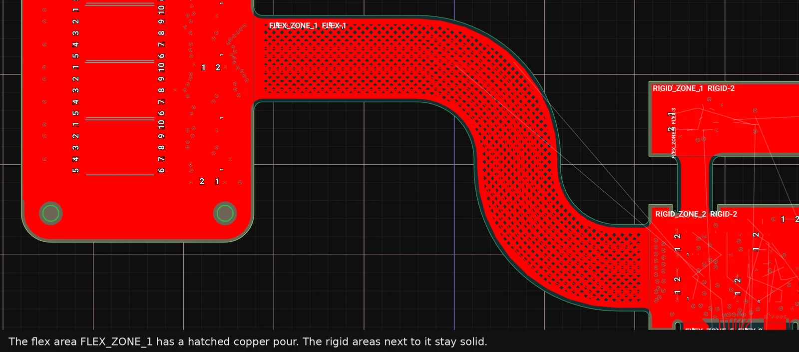
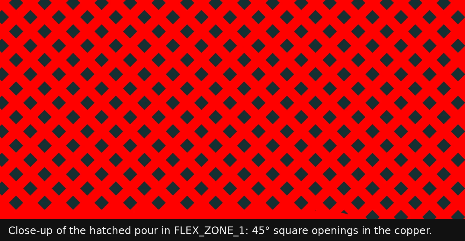
Hatched copper where the board bends
Solid copper is stiff. When a flex area bends, a solid copper pour can crack. A hatched pour is a grid of thin copper lines with open spaces between them. It bends without cracking.
Flux hatches the copper pours in flex areas and keeps the pours in rigid areas solid. The hatch lines are 0.25 mm wide with a 0.5 mm gap, at 45°. A 0.5 mm solid border runs along the edge of the pour, and solid rings stay around pads and vias of the same net.
See it in 3D. Send it to the mechanical team.
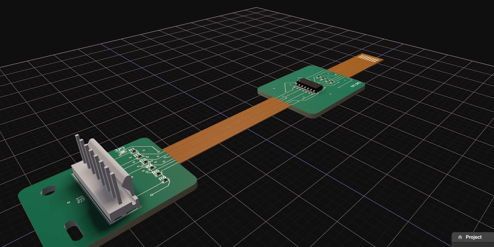
The 3D view shows each area at its own thickness. Download the board in 3D and give it to the team that designs the frame and the housing.
Bend it, twist it, fit it
You or the agent add a Flex Joint to a flex Stackup Area. On a pure-flex board, the Flex Joint goes directly on the board. A Flex Joint has two optional rules, Bend and Twist. Set one or both.
- Bend, for example
90deg 1mm, sets the bend angle and the bend radius. The longhand rules are Bend Angle and Bend Radius. - Twist, for example
90deg 20mm, sets the twist angle and the twist length. The longhand rules are Twist Angle and Twist Length. - Position, Rotation and Repeated Bending complete the Flex Joint.
Flux shows the bend zone on the board and the folded board in the 3D view. The 3D downloads are folded too. Put the folded board in the enclosure in the 3D view and check that it fits.
The design checks know bends. They compare the bend radius with the minimum for the flex stackup, which is larger for repeated bending. They check the minimum twist length for the width of the tail. They report parts, pads, vias and holes in a bend or twist zone, traces that do not cross a bend at 90°, and zones that overlap.
Ask the agent:
Fold the camera tail 90° at the hinge with a 1 mm bend radius, then check that the board fits in the frame.
Twist the tail 90° over 20 mm, so that the connector faces the main board.
Ready for the fab
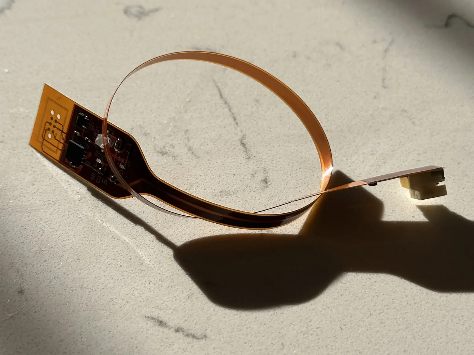
The manufacturing files carry the Stackup Areas. Gerber files include the coverlay and stiffener layers and a fabrication drawing that shows each area with its stackup. IPC-2581 and ODB++ exports include the Stackup Areas too.
In your Flux project, get quotes for flex boards from JLCPCB and PCBWay, and quotes for rigid-flex boards from PCBWay. Order flex boards from JLCPCB. PCBWay gives the rigid-flex price after it reviews the files.
Try it
Open a project in Flux and ask the agent for a flex or rigid-flex board. Earbuds, a wearable, a camera module, a sensor that wraps around a pipe.
Rigid where the parts sit. Flex where the board must move. One project, one agent.
FAQs
Yes. Set a bend angle and radius at a bending line. The PCB editor shows the flat board and its bend zones. The 3D view shows the folded board, and 3D downloads use the folded shape.
Yes. Each area stackup selects layers from one ordered layer list. A flex area can use inner rigid layers such as L3 and L4. The layers keep the same name, number, and Z position, so traces continue on the same physical layers across the rigid-to-flex boundary.
Put the folded board in the enclosure in the 3D assembly to check fit and clearance. Change the bend angle or radius until the board fits.
Yes. The 3D downloads show the folded board. Export it as a STEP file for mechanical design.
Yes. Flux routes each net only on the layers of the areas it crosses and does not place vias where an area stackup does not allow them. Ask Flux to route the whole board or selected groups of nets, fan out a BGA, route differential pairs at a target impedance, or tune lengths to a tolerance.
Flux supports layer continuity, area stackups, bending lines, folded 3D views, enclosure fit checks, and routing in one workflow. See the Flux vs Altium comparison.
Related Content

Circle it. Ask Flux. Markup mode is here

AI Moving a Mouse in Altium Is the Worst Way to Design a PCB

Your PCB Fabrication Drawing Now Comes From the Design

The Future of AI Isn't Better Prompting. It's Agents That Drive Their Own Work.

AI Gives You the Power of an Entire Supply-Chain Team

Streamline Component Research with AI
Let’s start building.

Let’s build your idea together. All you need to do is describe what you want to make, or what problem you want to solve. Flux will work with you to make it a reality.
