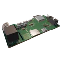
ESP32-S3 Schematics
The ESP32-S3 is Espressif's dual-core Xtensa LX7 microcontroller with 2.4 GHz Wi-Fi and Bluetooth 5 (LE). It adds vector instructions for AI and signal-processing workloads, native USB OTG, and up to 45 programmable GPIOs, making it a popular choice for camera, display, voice, and other edge AI devices. Common modules and boards include the ESP32-S3-WROOM-1, ESP32-S3-MINI-1, ESP32-S3-DevKitC-1, and the Seeed Studio XIAO ESP32-S3. They are used in smart home controllers, wearables, HMI panels with SPI or RGB displays, and battery-powered IoT sensors. Flux.ai has a large community-driven public library of ESP32-S3 parts, modules, and reference designs, with footprints, symbols, datasheets, and 3D models, so you can drop the ESP32-S3 into a schematic and PCB and start designing right away.

Jiji v3
ESP32-S3 CAM Audio-Visual Controller with I2S MEMS Microphone, Class-D Amplifier, SPI Display, Servos, Capacitive Touch and Integrated USB-C Power-Only Sink (VBUS via J6 -> 5V_IN -> SW1:P1 -> 5V_SW, CC1/CC2 5.1 kOhm to GND, VBUS TVS Surge Protection) + Added optional bulk electrolytic caps on 5V_SW near servo headers
0 Uses0 StarsESP32-S3-DEVKITC-1-N16R8V
ESP32-S3-DEVKITC-1-N16R8V is an Espressif ESP32-S3-DevKitC-1 v1.1 development board based on the ESP32-S3-WROOM-2-N16R8V module. It provides dual-core ESP32-S3 processing, 2.4 GHz Wi-Fi, Bluetooth LE, 16 MB Octal SPI flash, 8 MB Octal SPI PSRAM, USB programming/debugging, native USB OTG/JTAG capability, onboard power regulation, and two 22-pin 2.54 mm header rows for prototyping. Note: on this WROOM-2/N16R8V variant, GPIO35, GPIO36, and GPIO37 are used internally for Octal SPI flash/PSRAM and are not available for external use; GPIO38 drives the onboard RGB LED on v1.1 boards.
59 Uses0 StarsCoffee Waker Main HQ W/ Module V5.0.1 1243 f1b0 4389
Multi-subsystem ESP32-S3 coffee maker/alarm controller board for a Coffee Waker appliance. The design uses an ESP32-S3-WROOM-1-N8R8 module as the main Wi-Fi/Bluetooth MCU, with USB-C 2.0 device connectivity through a USB4105-GF-A connector, 5.1 kΩ CC pull-downs, and USBLC6-2SC6 ESD protection on the USB D+/D− pair. Power architecture includes a 12 V input on a JST VH B4P connector, a TPS62932 buck regulator generating the 5 V rail, a TLV1117LV33 3.3 V LDO for MCU/logic power, and TPS22919 load switches for controlled 3.3 V/5 V peripheral rails. Functional blocks include an NAU7802 load-cell ADC on I2C with two differential load-cell channels, a MAX98357A I2S audio amplifier/DAC with speaker/output filtering, a microSD socket on SDIO, I2C/test headers, UART/programming header, and auxiliary JST VH connectors for wake-light or external loads. The high-voltage section includes 120 VAC input/output screw terminals, a 5 V SPST-NO relay rated 15 A / 240 VAC max, a 1 A fuse, MOV surge suppression, diode snubber, and a dedicated heater output terminal.
0 Uses0 Stars